[nextpage title=”Introduction”]
Until the release of the AGP bus, video cards were installed in the PCI bus. The maximum theoretical transfer rate of the 32-bit PCI bus at 33 MHz was 133 MB/s, an insufficient rate for 3D applications (such as games, for instance) and that limited the development of more sophisticated video cards. Besides of its low transfer rate, the PCI bus had another problem: it was “choked”. The chipsets architecture used at that time was that of bridges, which used the PCI bus for the communication of the north bridge circuit with the south bridge one. Besides, most on-board peripherals of the PC were installed in the PCI bus, such as the on-board IDE ports, the SCSI controller, the on-board video, sound and network cards. No to mention the peripherals that could be installed in the PCI bus via PCI slots.
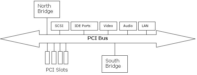 Figure 1: Simplified diagram of the PCI bus.
It happens that the maximum transfer rate of the PCI bus – 133 MB/s – is shared by devices connected to the bus, and not used by each peripheral during its transfer. In other words, the transfer rate used by a PCI video card is not 133 MB/s, but lower, for the more peripherals plugged to the PCI bus, the lower will the real transfer rate obtained by them be.
Motivated by those reasons, Intel launched the AGP bus. The main aim of the AGP bus was to increase the transfer rate of the video cards – having them installed in the faster AGP bus and no longer in the PCI bus. Technically speaking, AGP is not a bus, for only one device is connected to it: the video card. It is more a high performance point-to-point connection used only by video cards.
Intel launched the first version of the AGP (Accelerated Graphics Port or Accelerated Graph Port) bus in July, 1996. That bus worked with a clock of 66 MHz transferring 32 bits at a time, it was fed with 3.3V and operated in two modes: 1x and 2x. The first chipset to support such bus was the Intel 440LX, marketed in August, 1997.
In May, 1998, Intel launched the second version of the AGP bus that allowed the operation mode at 4x and was fed with 1.5V. The first chipset to support the second version of the ACP bus was the Intel 815P, marketed in June, 2000.
The most recent version of the AGP bus is the third one, developed in November, 2000. Actually it is an enhancement of the second version, allowing the operation mode at 8x. The first chipset to support the third version of the ACP bus was the Intel 865P, marketed in May, 2003.
| Version | Operation Modes | Voltage |
| AGP 1.0 | 1x and 2x | 3.3v |
| AGP 2.0 | 1x, 2x and 4x | 1.5V |
| AGP 3.0 | 1x, 2x, 4x and 8x | 1.5V |
[nextpage title=”Operation Modes”]
The operation modes of the AGP bus refer to the amount of data that are transferred by clock cycle. The 1x AGP is capable of transferring only one datum per clock tick. Since the AGP bus works at 66 MHz (66.66 MHz to be exact), transferring 32 bits of data at a time, the maximum transfer rate of the 1x AGP bus is 266 MB/s, twice as much as that of the PCI bus. The 2x AGP bus works transferring two data per clock cycle, which results in a transfer rate of 533 MB/s. The second version of the AGP bus introduced the 4x operation mode, which allows transferring four data per clock cycle, obtaining then a transfer rate of 1,066 MB/s. The newest video cards allow operating in the 8x mode, which has a transfer rate of 2,133 MB/s, sixteen times higher than that of the PCI bus!
| Mode | Clock | Number of bits | Data per clock cycle | Transfer Rate |
| x1 AGP | 66 MHz | 32 bits | 1 | 266 MB/s |
| x2 AGP | 66 MHz | 32 bits | 2 | 533 MB/s |
| x4 AGP | 66 MHz | 32 bits | 4 | 1,066 MB/s |
| x8 AGP | 66 MHz | 32 bits | 8 | 2,133 MB/s |
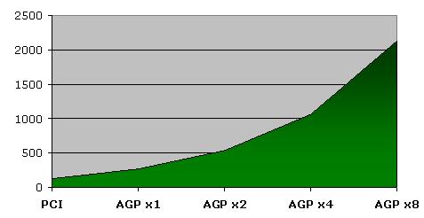
Figure 2: Comparison between the transfer rates of the PCI bus and the AGP bus.
Besides working at high transfer rates, the AGP bus also allows the video card to use the RAM memory of the PC as an extension of its video memory, for the storage of textures and the z-buffering (responsible for the depth vector in 3D images), which considerably increases its performance, since the memory bus is faster than the AGP bus. That resource is known as DIME (Direct Memory Execute) or AGP Texturing and is not supported by all AGP video cards.
[nextpage title=”Slot Types”]
AGP video cards working at 1x or 2x modes are fed with 3.3V, while x4 and x8 video cards are fed with 1.5V. The first motherboards with AGP slots allowed only the installation of AGP video cards fed with 3.3V. If you installed a 1.5 V AGP board in one of those old motherboards, which only had 3.3V output, both the video card and the motherboard could burn! To avoid such type of problem, the AGP bus specification defined three types of slots: one, called Universal, allows both 1.5V and 3.3V boards to be installed; another one that only allows 3.3 V boards to be installed; and another one that should only be used by 1.5 V video cards.
In August, 1998 a new specification of the AGP bus was launched: AGP Pro. AGP Pro defined a larger slot, with more voltage pins, for high-consumption 3D video cards. The AGP Pro slot is compatible with the previous versions of the AGP bus, in other words, you can install conventional 1.5 V or 3.3 V AGP video cards in AGP Pro slots.
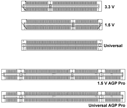
Figure 3: Types of AGP slots.
Figure 4: 1.5 V AGP card being installed in a 1.5 V AGP slot.
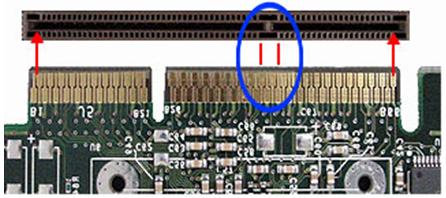
Figure 5: It is not possible to install a 3.3 V video card in a 1.5 V AGP slot.
Leave a Reply